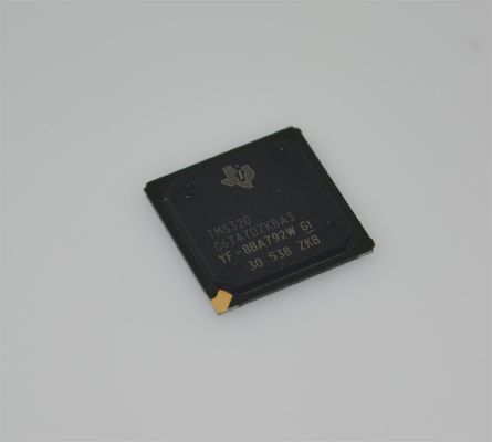
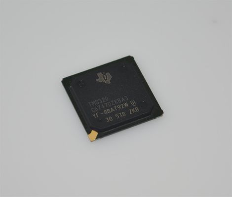
TMS320C6747DZKBA3 456MHz Dual-Core DSP 3648MBPS 32KB L1 Cache 256KB RAM BGA-256 -40anddeg;C to +100anddeg;C Industrial DSP
andnbsp;
Features andnbsp;
andbull; Software Support
andndash; TI DSP/BIOSandtrade;
andndash; Chip Support Library and DSP Library
andbull; 375- and 456-MHz TMS320C674x VLIW DSP
andbull; C674x Instruction Set Features
andndash; Superset of the C67x+ and C64x+ ISAs
andndash; Upto 3648 MIPS and 2736 MFLOPS C674x
andndash; Byte-Addressable (8-, 16-, 32-, and 64-Bit Data)
andndash; 8-Bit Overflow Protection
andndash; Bit-Field Extract, Set, Clear
andndash; Normalization, Saturation, Bit-Counting
andndash; Compact 16-Bit Instructions
andbull; C674x Two-Level Cache Memory Architecture
andndash; 32KB of L1P Program RAM/Cache
andndash; 32KB of L1D Data RAM/Cache
andndash; 256KB of L2 Unified Mapped RAM/Cache
andndash; Flexible RAM/Cache Partition (L1 and L2)
andbull; Enhanced Direct Memory Access Controller 3 (EDMA3):
andndash; 2Transfer Controllers
andndash; 32Independent DMA Channels
andndash; 8Quick DMA Channels
andndash; Programmable Transfer Burst Size
andbull; TMS320C674x Fixed- and Floating-Point VLIW DSP Core
andndash; Load-Store Architecture with Nonaligned Support
andndash; 64General-Purpose Registers (32-Bit)
andndash; Six ALU (32- and 40-Bit) Functional Units
andndash; Supports 32-Bit Integer, SP (IEEE Single Precision/32-Bit) and DP (IEEE Double Precision/64-Bit) Floating Point
andndash; Supports up to Four SP Additions Per Clock, Four DP Additions Every 2 Clocks
andndash; Supports up to Two Floating-Point (SP or DP) Reciprocal Approximation (RCPxP) and Square-Root Reciprocal Approximation (RSQRxP) Operations Per Cycle
andndash; TwoMultiply Functional Units
andndash; Mixed-Precision IEEE Floating Point Multiply Supported up to:
andndash; 2SPxSP-andgt;SPPerClock
andndash; 2SPxSP-andgt;DPEvery Two Clocks
andndash; 2SPxDP-andgt;DPEvery Three Clocks
andndash; 2DPxDP-andgt;DPEvery Four Clocks
andndash; Fixed-Point Multiply Supports Two 32 x 32-Bit 1 Multiplies, Four 16 x 16-Bit Multiplies, or Eight 8 x 8-Bit Multiplies per Clock Cycle, and Complex Multiples
andndash; Instruction Packing Reduces Code Size
andndash; All Instructions Conditional
andndash; Hardware Support for Modulo Loop Operation
andndash; Protected Mode Operation
andndash; Exceptions Support for Error Detection and Program Redirection
andbull; 128KB of RAM Shared Memory (TMS320C6747 Only)
andbull; 3.3-V LVCMOS I/Os (Except for USB Interfaces)
andbull; TwoExternal Memory Interfaces:
andndash; EMIFA
andndash; NOR(8- or 16-Bit-Wide Data)
andndash; NAND(8- or 16-Bit-Wide Data)
andndash; 16-Bit SDRAM with 128-MB Address Space (TMS320C6747 Only)
andndash; EMIFB
andndash; 32-Bit or 16-Bit SDRAM with 256-MB Address Space (TMS320C6747)
andndash; 16-Bit SDRAM with 128-MB Address Space (TMS320C6745)
andbull; Three Configurable 16550-Type UART Modules:
andndash; UART0 with Modem Control Signals
andndash; Autoflow Control Signals (CTS, RTS) on UART0 Only
andndash; 16-Byte FIFO
andndash; 16x or 13x Oversampling Option
andbull; LCDController (TMS320C6747 Only)
andbull; TwoSerial Peripheral Interfaces (SPIs) Each with One Chip Select
andbull; Multimedia Card (MMC)/Secure Digital (SD) Card Interface with Secure Data I/O (SDIO)
andbull; TwoMaster and Slave Inter-Integrated Circuit (I2C Busandtrade;)
andbull; OneHost-Port Interface (HPI) with 16-Bit-Wide Muxed Address/Data Bus for High Bandwidth (TMS320C6747 Only)
andbull; Programmable Real-Time Unit Subsystem (PRUSS)
andndash; TwoIndependent Programmable Realtime Unit (PRU) Cores
andndash; 32-Bit Load and Store RISC Architecture
andndash; 4KBof Instruction RAM per Core
andndash; 512 Bytes of Data RAM per Core
andnbsp;
Applications
andbull; A/VReceivers
andbull; Automotive Amplifiers
andbull; Soundbars
andbull; HomeTheatre Systems
andbull; Professional Audio
andbull; Network Streaming Audio
andnbsp;
Description
The TMS320C6745/6747 device is a low-power digital signal processor based on a TMS320C674x DSP core. It consumes significantly lower power than other members of the TMS320C6000andtrade; platform of DSPs.
The TMS320C6745/6747 device enables original-equipment manufacturers (OEMs) and original-design manufacturers (ODMs) to quickly bring to market devices featuring high processing performance .
The TMS320C6745/6747 DSP core uses a two-level cache-based architecture. The Level 1 program cache (L1P) is a 32-KB direct mapped cache and the Level 1 data cache (L1D) is a 32-KB 2-way set associative cache. The Level 2 program cache (L2P) consists of a 256-KB memory space that is shared between program and data space. L2 memory can be configured as mapped memory, cache, or combinations of the two. Although the DSP L2 is accessible by other hosts in the system, an additional 128KB of RAM shared memory (TMS320C6747 only) is available for use by other hosts without affecting DSP performance.
andnbsp;
INFORMATION
|
Category
|
|
andnbsp;
|
|
Manufacturer
|
|
|
|
Series
|
|
|
|
Packaging
|
|
|
|
Part Status
|
|
|
|
Type
|
|
|
|
Interface
|
EBI/EMI, Ethernet MAC, Host Interface, I2C, McASP, SPI, UART, USB
|
|
|
Clock Rate
|
|
|
|
Non-Volatile Memory
|
|
|
|
On-Chip RAM
|
|
|
|
Voltage - I/O
|
|
|
|
Voltage - Core
|
|
|
|
Operating Temperature
|
-40anddeg;C ~ 105anddeg;C (TJ)
|
|
|
Mounting Type
|
|
|
|
Package / Case
|
|
|
|
Supplier Device Package
|
|
|
|
Base Product Number
|
|
andnbsp;
Drawing

Our advantage :
- High quality products --- our offers are 100% new and original, ROHS
- Competitive price --- good Purchase channels with good price.
- Professional service --- strict quality testing before the shipment, and perfect after-sales service after the purchase.
- Adequate inventory --- With the support of our strong Purchasing team,
- Fast delivery --- we will ship the goods within 1-3 working days after the payment confirmed.
andnbsp;
be sure to meet your need for all kinds of components. ^_^
Product List
Supply a Series of Electronic Components, full range of semiconductors, active andamp; passive Components.We can help you to get all for bom of the PCB,IN a word, you can get one-stop solution here,
The offers including:
Integrated Circuit, Memory ICs, Diode, Transistor , Capacitor, Resistor, Varistor, Fuse, Trimmer andamp; Potentiometer, Transformer, Battery, Cable, Relay, Switch, Connector, Terminal Block, Crystal andamp; Oscillator, Inductor, Sensor, Transformer, IGBT Driver, LED,LCD, Convertor, PCB (Printed Circuit Board),PCBA (PCB Assembly)
Strong in Brand:
Microchip, MAX, AD, TI, ATMEL, ST, ON, NS, Intersil, Winbond, Vishay, ISSI, Infineon, NEC, FAIRCHILD, OMRON,YAGEO, TDK, etc

 Your message must be between 20-3,000 characters!