Customized Medical Devices 2 OZ PCB Assembly Services PCBAandnbsp; Board
andnbsp;
andnbsp;
Description:
andnbsp;CCL-FR4
andnbsp;
Specifications:andnbsp;CCL-FR4 consists of E-glass fabric, impregnated with epoxy resin and clad with electrolytic foil 0.6mm,0.8mm,1.0mm,1.2mm,1.5mm,1.6mm.
andnbsp;
Characteristic and Application:andnbsp;FR4 Copper Clad Laminate/CCL consists of E-glass fabric, impregnated with epoxy resin and clad with electrolytic foil. It has excellent electric, mechanical and flamer retardant properties and is widely used for PWB with printed circuit on single or double side in microwave ovens, computers, computers, communication apparatus as well as other high grade electronic instruments.
andnbsp;
Normal Thickness:andnbsp;0.6mm , 0.8mm , 1.0mm , 1.2mm , 1.5mm , 1.6mm .
andnbsp;
Size Available:andnbsp;41*49
andnbsp;
andnbsp;
Specification:
|
Item
andnbsp;
|
Capabilities
andnbsp;
|
|
Number of Layers
andnbsp;
|
- Single-side ;
- Double Side;
- andnbsp;Multi-layer (4~22 Lay)
|
|
Material
andnbsp;
|
1. CEM-1, FR-2, FR-1 XPC-94HB
2. FR-4,CEM-3,HighTg, Aluminum,
Halogen Free
3. andnbsp;4 to 22 layers(FR-4, High Tg, Rogers)
|
|
PCB Thickness
andnbsp;
|
Min. thickness
andnbsp;
|
0.2mm(8mil)
|
|
Max. thickness
andnbsp;
|
3.2mm(128mil)
andnbsp;
|
|
Surface finished
andnbsp;
|
Gold Plating
andnbsp;
|
|
Immersion Gold(Silver)
andnbsp;
|
|
HAL Lead Free
andnbsp;
|
|
Hot Air Solder Leveling(HASL)
andnbsp;
|
|
Entek Coating (OSP)
andnbsp;
|
|
Solder Mask
andnbsp;
|
Green, White, Black, Yellow, Red, blue
andnbsp;
|
|
Other printing
andnbsp;
|
Gold Finger
andnbsp;
|
|
Carbon Print, Peelable Mask
andnbsp;
|
|
Solder Mask Plugged Hole
andnbsp;
|
|
Copper thickness
andnbsp;
|
0.5oz, 1oz, 2oz, 3oz,4oz
1/ 2 oz (18 andmu;m) - 4 oz (140 andmu;m)
andnbsp;
|
|
Min. Finished Hole Size
andnbsp;
|
0.3mm(12mil)
andnbsp;
|
|
Hole Size Tolerance (PTH)
andnbsp;
|
+/ -0.076mm (3 mil)
andnbsp;
|
|
Hole Size Tolerance (NPTH)
andnbsp;
|
+/-0.05mm (2 mil)
andnbsp;
|
|
Min. Line Width and Spacing
andnbsp;
|
0.10mm (4 mil)
andnbsp;
|
|
Min. Solder Mask Clearance
andnbsp;
|
0.076mm (3 mil)
andnbsp;
|
|
Min. Annular Ring
andnbsp;
|
0.1mm (4mil)
andnbsp;
|
|
Profile and V-Cut
andnbsp;
|
CNC-Routing, Stamping and Beveling, V-CUT,CNC
andnbsp;
|
|
Special Process
andnbsp;
|
Micro-section, Chamfer for Gold Finger
andnbsp;
|
andnbsp;
andnbsp;
andnbsp;
Primary competitive advantages:
Profound knowledge of contract manufacturing services
Capable of developing effective production process to ensure high-quality and consistency
Experienced logistics management
Cost-effective factory located in mainland China
- Able to handle small as well as large volume production with flexibility
- We also had launched six Sigma DMAIC program since January 2002
- Our building products experience range: industrial, automotive, computing, storage, consumer, instrumentation, medicals, networking, peripherals and tele communications
andnbsp;
Application:
andnbsp;
The PCBs are used for wide range of electronic products:
Such as andnbsp;Medical devices, Military equipment ,autos mobile ,CCTV, Power supply, GPS, UPS, Set-top Box, Telecommunicationandnbsp;,LED, etc.
andnbsp;
andnbsp;
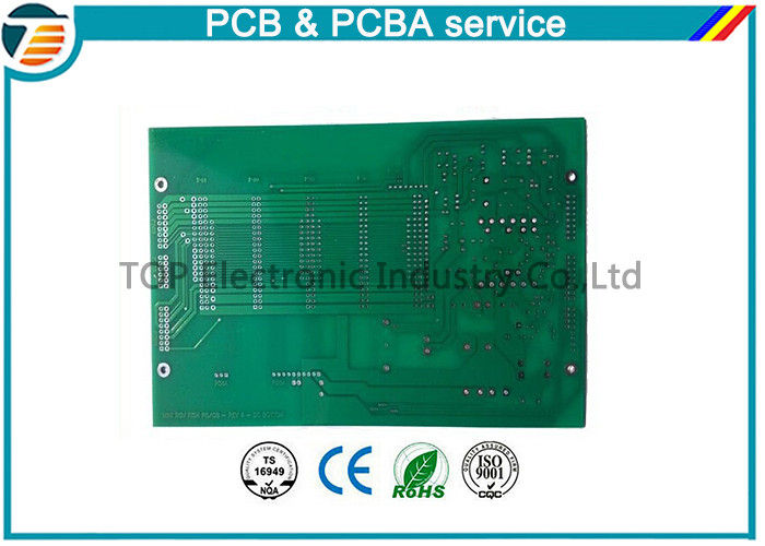
PCB show:

andnbsp;
The PCB factory which we cooperated has more than 14 yearsandnbsp;of Experience in PCB Industry,
There are more than 600 employees and four factories; one factory for prototypes, one for mass production, one for aluminum and copper PCBs, and one for PCB assembly. Each factory has the ability to make 8,000 square meters per month and we offer 1,000 kinds of PCB fabrication monthly, including one- to 20-layer PCBs, HDI, aluminum, heavy copper and halogen-free PCBs.
andnbsp;
we haveandnbsp;Double-sided cooperation with the PCB factory,our company offer them a series electronic components and other parts for BOM, and we make PCB and assembly there.so both of us can get veryandnbsp;competitive price.
andnbsp;
With the powerful support from the partner, weandnbsp;Have confidenceandnbsp;to give our customers best service.

 Your message must be between 20-3,000 characters!